01
Microfabrication
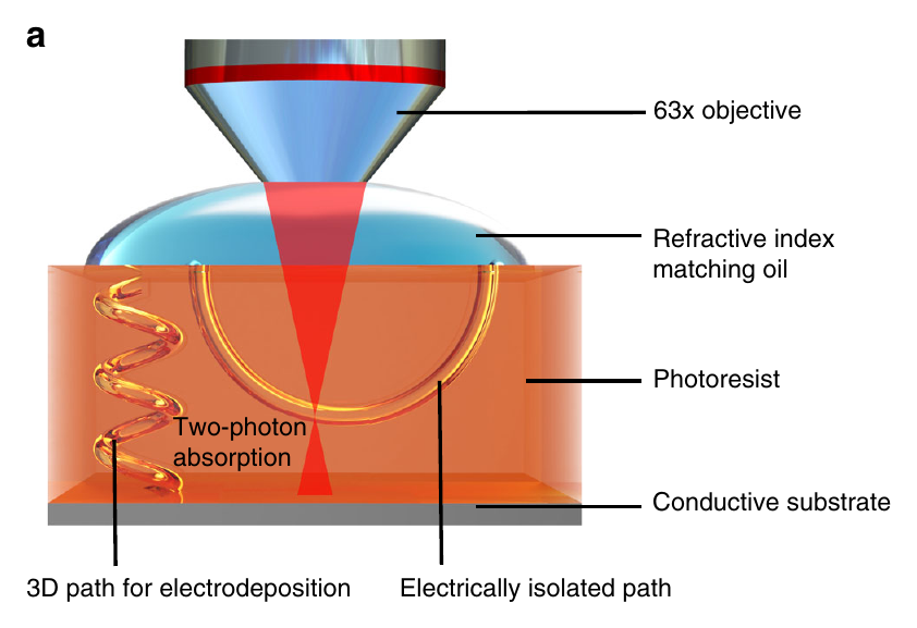
My fabrication work has included lithography, 3D microfabrication, mold casting, electrodeposition, and thin-film deposition.
PhD, ETH Zurich
Staff Engineer, Samsung Electronics
Currently based in South Korea
My work has focused on turning designs into working physical systems. So far, that has meant microrobots at ETH Zurich, machine vision for robots in semiconductor manufacturing, and CMOS-integrated devices for cellular and neural sensing, along with applied AI for image and signal analysis.
01
01
My fabrication work has included lithography, 3D microfabrication, mold casting, electrodeposition, and thin-film deposition.
02
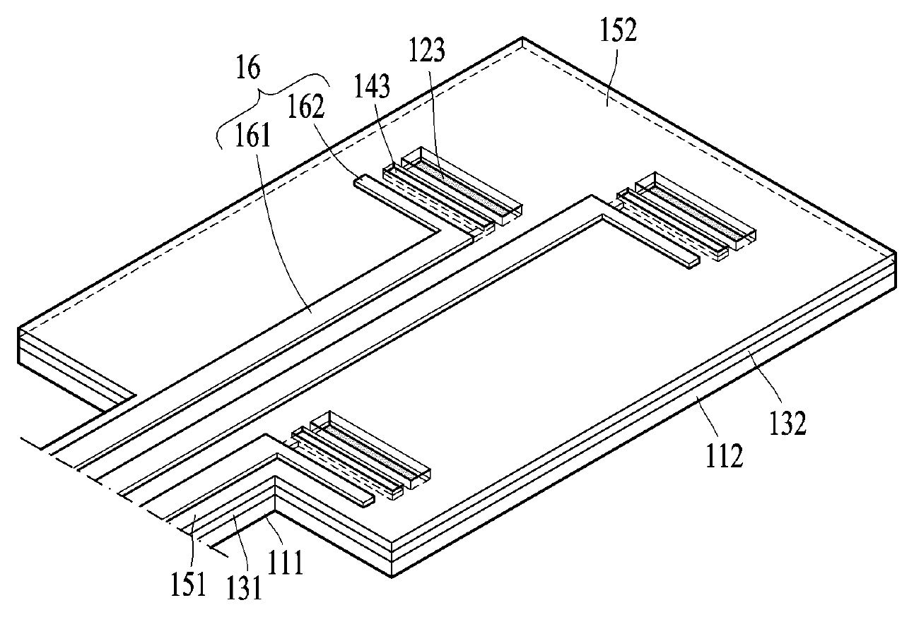
I have worked on physical interfaces including CMOS-integrated electrodes and devices for cellular and neural sensing.
03
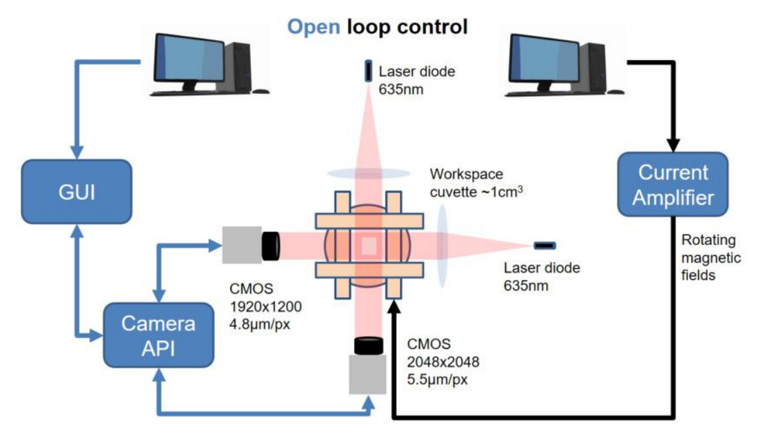
I have developed perception systems for robotic manipulation, including machine vision and automated data workflows. My earlier research also included untethered microrobots.
04
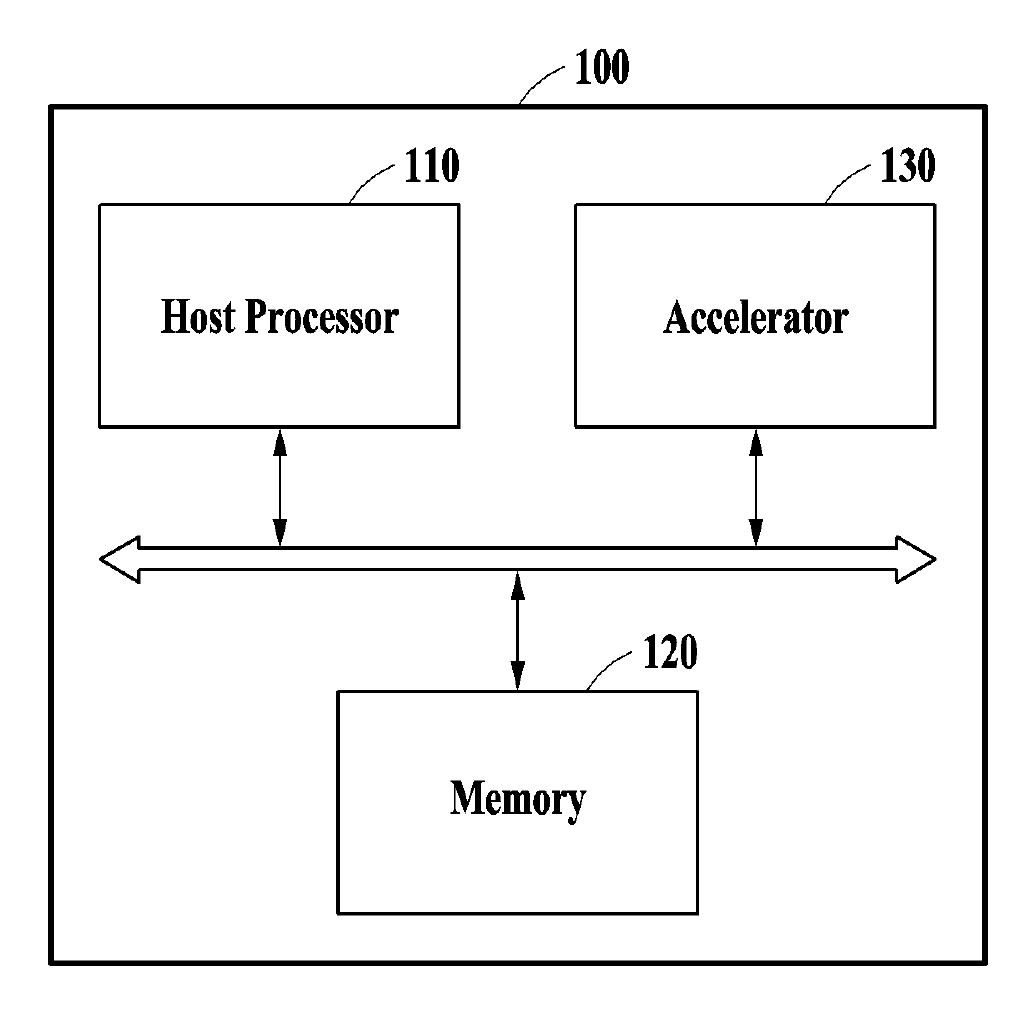
I have worked on AI for physical systems, including image and signal analysis, neural-network operations, and defect detection.
02
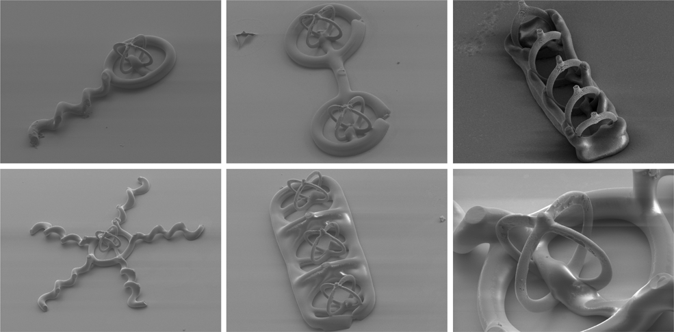
Co-first and corresponding author
A fabrication strategy for independently movable metallic, polymeric, and hybrid components at the microscale. I designed and fabricated the structures.
Covered by ETH Zurich and 3D Printing Industry
Read the paper


03
Applications on which I am a named inventor, with the assignee shown for each record.
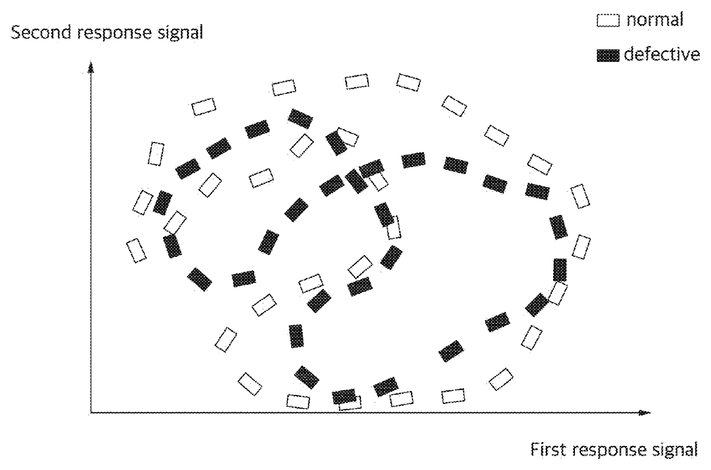
Defect detection, neural-network operations, and hardware emulation for physical inspection and compute systems.
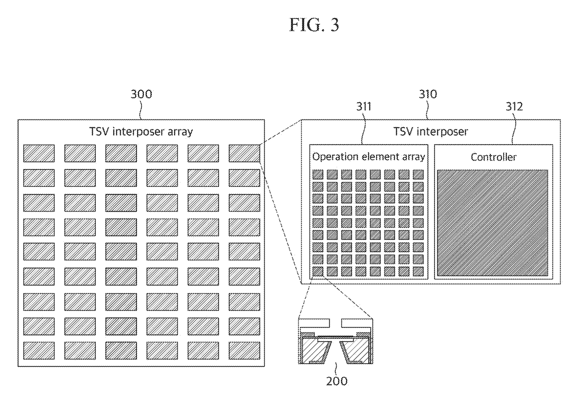
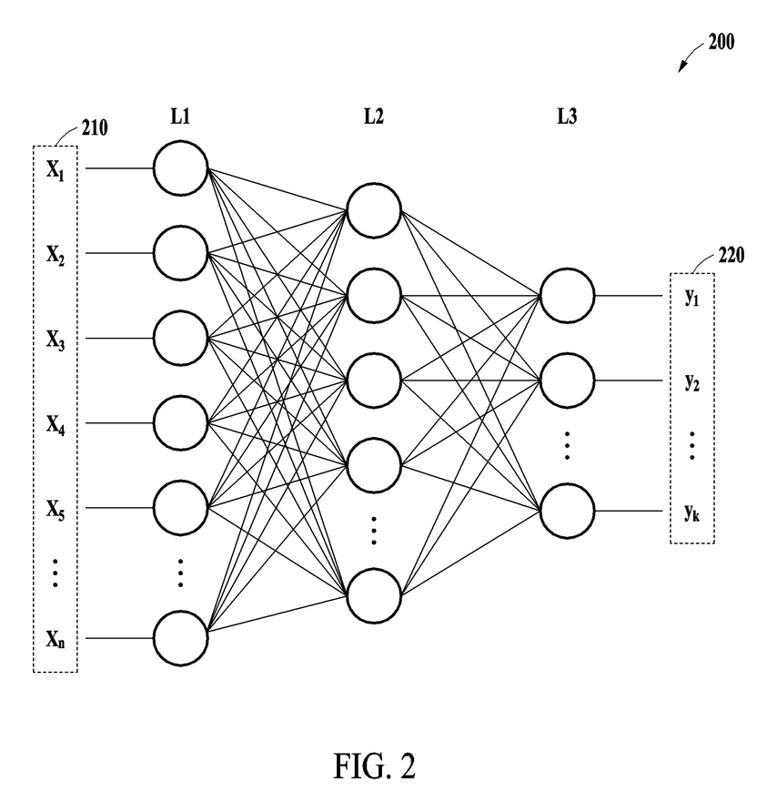
US20260094027A1
AI and compute
Second-listed inventor
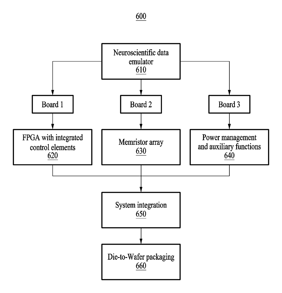
US20250335223A1
AI and compute
First-listed inventor
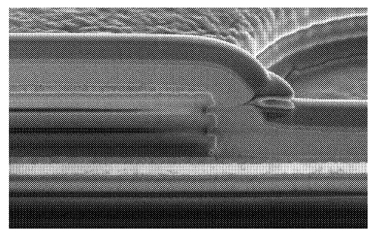
Electrode architectures and probes built around CMOS integration and cellular or neural signals.
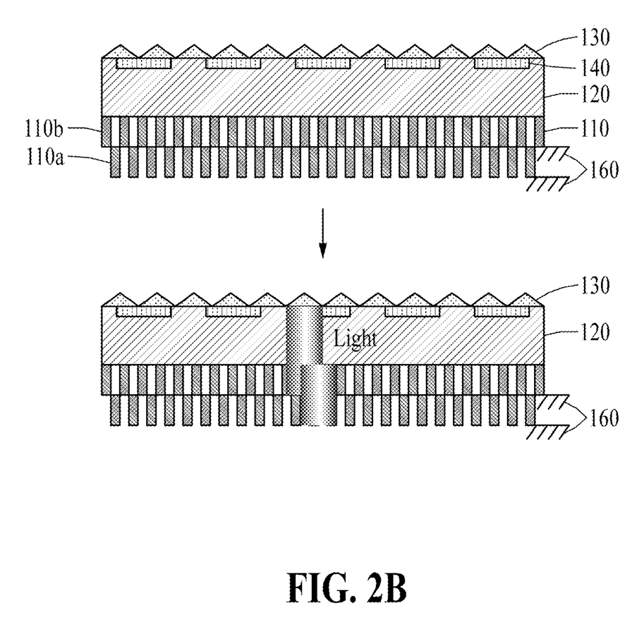
US20250189477A1
Sensing and devices
First-listed inventor
Granted in Europe as EP4568455B1, 2026
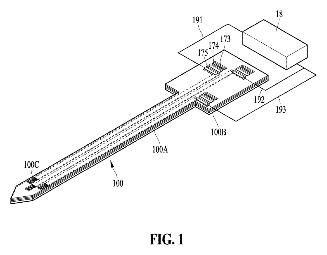
US20250194980A1
Sensing and devices
Third-listed inventor
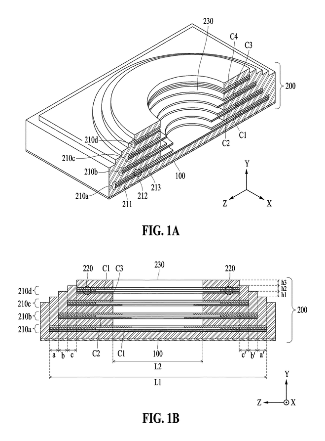
US20240290848A1
Sensing and devices
First-listed inventor
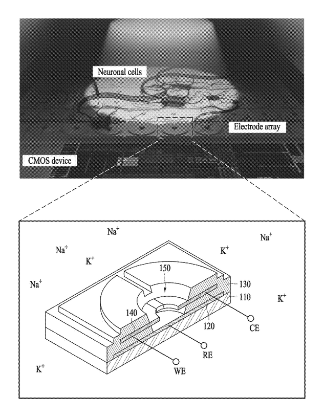
US20240393326A1
Sensing and devices
First-listed inventor
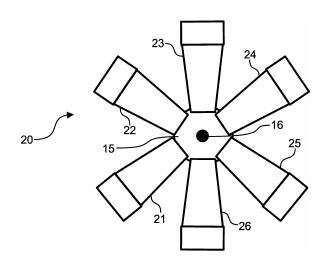
Monitoring and control concepts for phacoemulsification systems used in ophthalmic procedures.
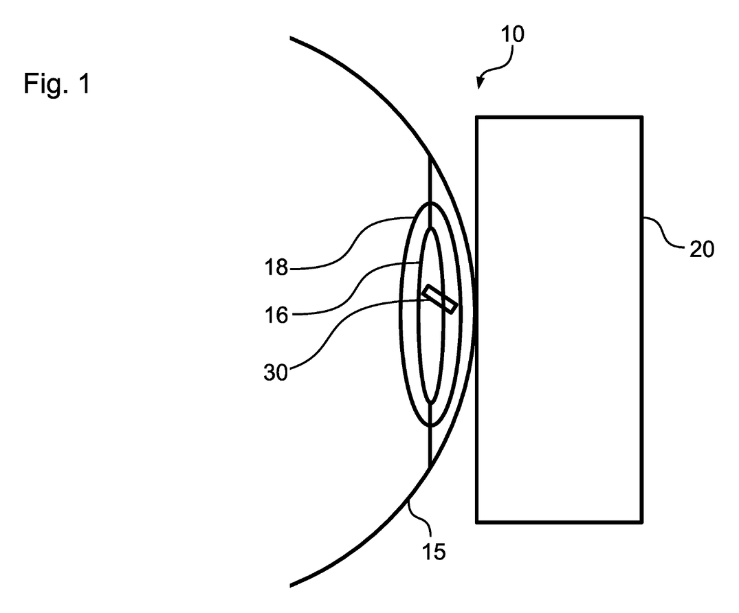
WO2022223172A1
Medical systems
Co-inventor
04
2022 - present
Staff Engineer
I developed CMOS-integrated sensing devices across system specification, materials integration, and fabrication. I also deployed AI models for signal analysis.
2020 - 2022
Staff Engineer
I developed machine-vision systems for real-time robotic manipulation in semiconductor manufacturing, including ML workflows for automated data acquisition and annotation.
2015 - 2019
Research Assistant
I designed and fabricated metallic, polymeric, and hybrid microrobots using lithography, direct laser writing, mold casting, electrodeposition, and thin-film deposition.
2013 - 2015
Research Assistant
I studied thiol adsorption on gold surfaces using surface plasmon resonance and worked with thin-film fabrication and characterization.
2011 - 2012
Engineering Internships
I developed a wireless power transfer prototype at ABB, a fault-detection method for induction motors at Siemens, and a database interface for magnetic-measurement data at CERN.
Ideas / Research / Shared interests
If something here connects with your work, a paper you are reading, or an idea you are exploring, I would be happy to hear from you.
alcantara at ccjalcantara.com